
Temperature Control Solutions in the Semiconductor Industry
Today, every smartphone contains millions of times more computing power than NASA had available for the Apollo missions. We owe this to the semiconductor industry, which is accommodating more and more power in smaller and smaller spaces while pushing the limits of what is technically and physically feasible. High-precision procedures are used to build complex circuits that are only visible at high magnification. In the semiconductor industry, there is very little room for error in the truest sense of the word. Numerous process steps are linked to a precise temperature control application.
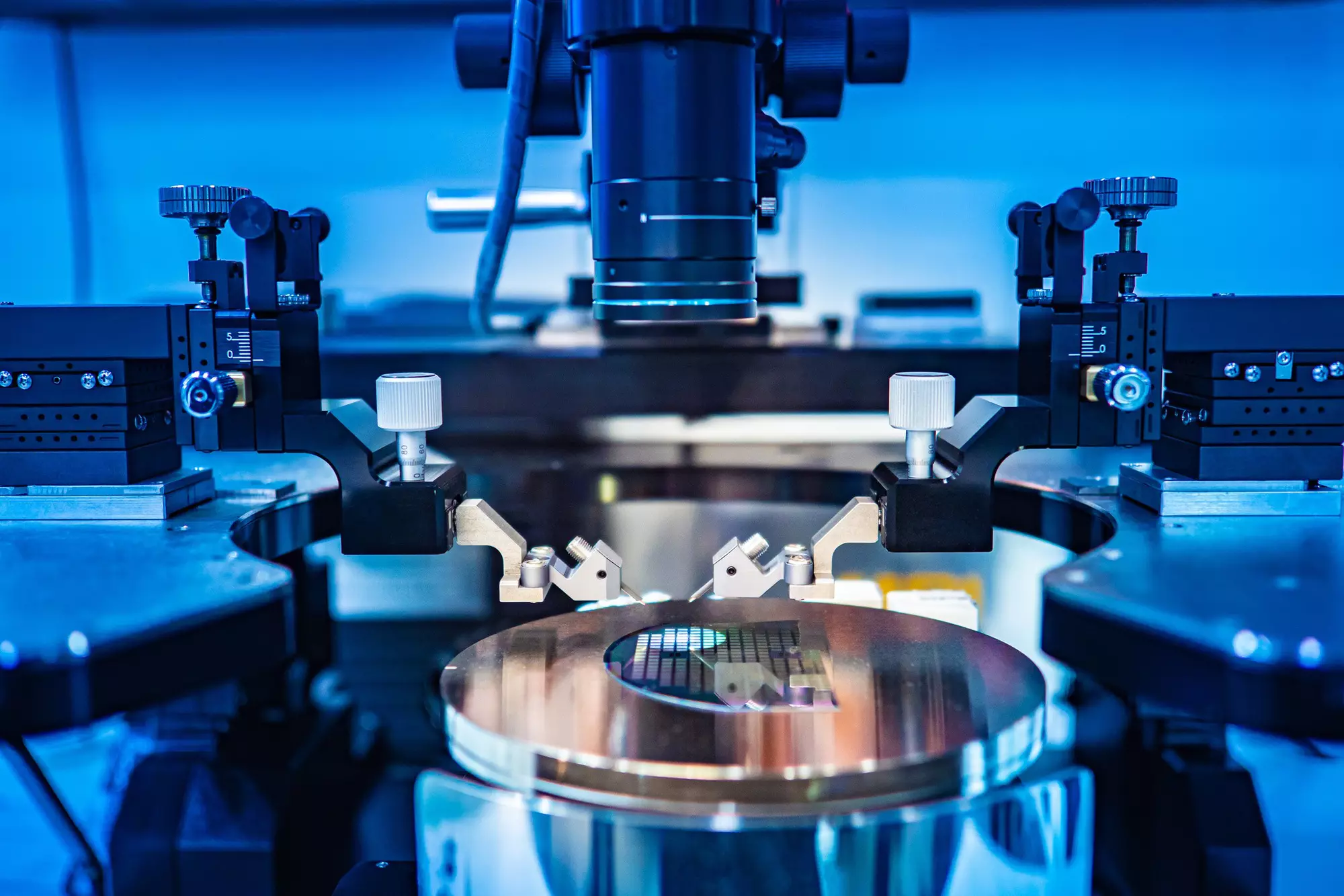
The Wafer - The Backbone of the Modern World
In today's everyday life, there is virtually nothing left that can do without sophisticated control electronics. Semiconductor-based components form the basis of this modern world. They are built on thin wafers made of mono- or polycrystalline semiconductor blanks (ingots). Technology companies usually use silicon wafers with a diameter of 300 mm and a thickness of 0.9 mm as a base plate for the production of microcircuits, which are contained in processors, flash memories, and RAMs, among other things. Several hundred processors, for example, are manufactured in parallel on these wafers, which are only separated from each other at the end of production. In modern processors, about one billion transistors fit on the surface of a fingernail. Conventional wiring and soldering techniques have therefore long ceased to be used in manufacturing. Instead, high-precision microchemical processes are used to build the circuits in extremely thin individual layers.
Process Methods in the Semiconductor Industry using Microchips as an Example
In very simplified terms, many identical integrated circuits are applied to a wafer using different coating, exposure, diffusion, doping, and etching processes. Conductive layers are applied and masked with a photosensitive resist. The resist undergoes a chemical change as a result of exposure to light. The exposed areas can thus be removed using a wet chemical etching process. The remaining photoresist mask is then transferred to the underlying layers using a dry etching process, for example. The resulting trenches in the material are then filled with non-conductive materials (mostly oxides). Oxide protrusions must then be precisely removed so that the contact surfaces are exposed again for further processing. This is followed by the next layer. As mentioned: very simplified.
In reality, for example, countless intermediate layers are being applied, which only serve to protect the underlying layers as a kind of stop layer in some processes. Once they have fulfilled their purpose, their residues must be removed again. The lowest layer of the microchip also consists of extremely thin paths of semiconductor material, which are given different conductivities (P and N material) by targeted contamination (doping), so that the current flow can be controlled by applying a supply voltage.
In this layering process, over 10 km of conductive paths, some of which are only a few atom layers high and wide, are created in around three months and approx. 1500 work steps (including defect inspection and test procedures) on a wafer with a diameter of 300 mm.
The accuracy of the surface treatments is in the range of less than one nanometer, which corresponds to only a few atomic layers. This can only be achieved by precise and 100 % reproducible processes in which all factors are precisely regulated. Approximately a quarter of the basic processes are wet chemical process steps.
Temperature Control Application of Wet Chemical Etching Baths in the Semiconductor Industry
In wet etching, solid material is liquefied by a chemical solution. The solutions used are matched to the coating material to be removed so that they are highly selective.
The etching rate (material removal per time) must be known down to the smallest detail and remain constant for as long as possible to achieve precision in the nanometer range. In addition, the reaction products must be dissolved immediately so as not to contaminate the etching solution. However, due to the reaction partners dissolved in the etching solution, its concentration also decreases with an increasing amount of processed wafers, which is why it must be replaced regularly. In addition to the concentration, the temperature of the etching bath, in particular, has a direct influence on the etching rate since chemical solutions usually become more reactive as the temperature rises. In addition, the temperature influences how quickly the reaction products dissolve.
The temperature of the etching baths thus plays a central role in the semiconductor industry. Minimal temperature deviations of the etching bath can already have catastrophic consequences and render an entire lot of wafers unusable. Therefore, only high-precision and fail-safe temperature control systems are used in wet-chemical processing. They must be able to keep the temperature within the target range with accuracy and react quickly to temperature deviations. In addition, they must quickly restore the correct temperature of the etching bath when the etching solution is replaced to ensure a constant production flow.
Conclusion
The production of conductive paths that make a human hair look like a bulwark requires absolute precision in the nanometer range. For this purpose, numerous processes in semiconductor production must be precisely temperature-controlled. In an almost infinite number of individual steps, extremely thin layers are applied, partially masked and the unmasked parts removed with absolute precision. The etching baths must be kept within an optimum temperature range to keep the etching rate constant and predictable in wet-chemical processes. This requires the use of absolutely precise and reliable temperature control solutions, which are ideally calibrated for the respective area of application.
A perfectly balanced temperature control system not only improves production results, but also increases process reliability and reduces production time, costs, and maintenance. Our experienced and well-rehearsed team of specialists in the field of temperature control of processes in the semiconductor industry will be pleased to answer your questions. Of course, we adapt our temperature control solutions to your individual needs if required.
